
This blogpost would not have been possible without the research conducted by Neel Gude, Research Analyst Intern at Speciale Invest, whose effort significantly shaped its content.
In the world of semiconductors, a lot of attention goes to chip architecture, manufacturing scale-ups, or which companies are pushing the boundaries of performance. But behind all of that is a quiet, critical process that makes modern chips possible: LITHOGRAPHY.
Lithography is the technique that allows chipmakers to etch billions of tiny transistors onto a fingernail-sized slice of silicon. It defines how small, how fast, and how energy-efficient a chip can be, by determining the size and density of the features on a wafer. This is done by transferring intricate patterns onto the wafer using a light-sensitive material called photoresist. This step directly impacts a chip’s performance, power efficiency, and production cost.
It’s a decades-old technology, but it’s still evolving fast and remains a key bottleneck in how small, powerful, and efficient chips can get.
The Two Lithography Techniques That Dominate Today
While there are many experimental and legacy techniques out there, two types of lithography dominate modern chip manufacturing; they are Deep Ultraviolet (DUV) and Extreme Ultraviolet (EUV) Lithography.
DUV lithography is the long-standing workhorse of the industry. It uses 193 nm ultraviolet light, typically from argon fluoride lasers, to print patterns onto silicon wafers. This technique supports nodes in the 28–90 nm range, which are still widely used in chips for automotive systems, industrial controllers, networking hardware, and many IoT devices. Despite being an older technology, DUV remains far more commonly used across global fabs due to its maturity, reliability, and relatively lower cost. A high-end DUV immersion tool typically costs $40–60 million, and major suppliers include ASML, Nikon, and Canon.
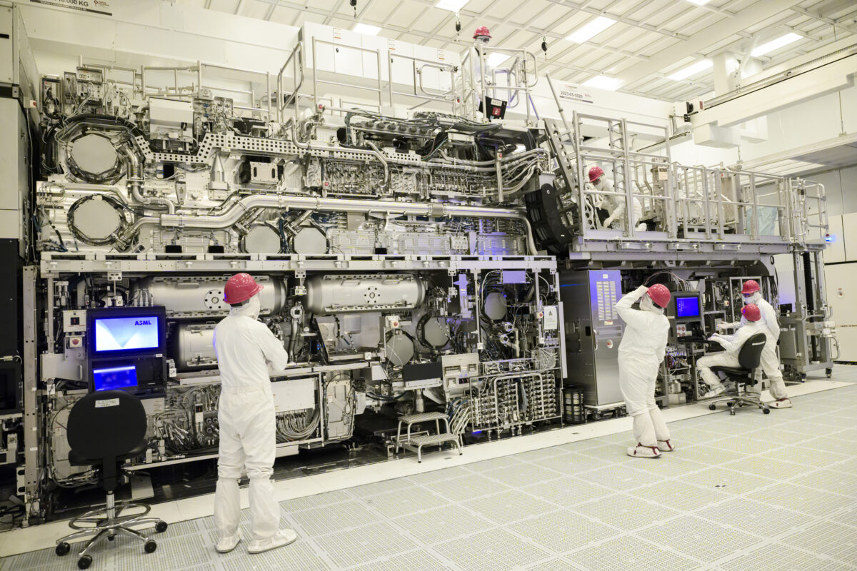
EUV lithography on the other hand is used to manufacture the world’s most advanced chips. It operates at a much shorter wavelength of 13.5 nm and is generated using laser-pulsed tin plasma. The process relies on highly specialized mirrors and vacuum chambers to focus the beam precisely. EUV is required for building chips at 7 nm and below, which power AI accelerators, high-performance computing systems, and premium mobile processors. While EUV allows for fewer patterning steps and higher transistor density, it comes at a cost: each machine can run between $150–180 million, and upcoming High-NA EUV tools are expected to exceed $300 million per unit. Currently, ASML is the only company in the world that manufactures EUV systems at scale.
Source: https://www.kbvresearch.com/lithography-equipment-market/
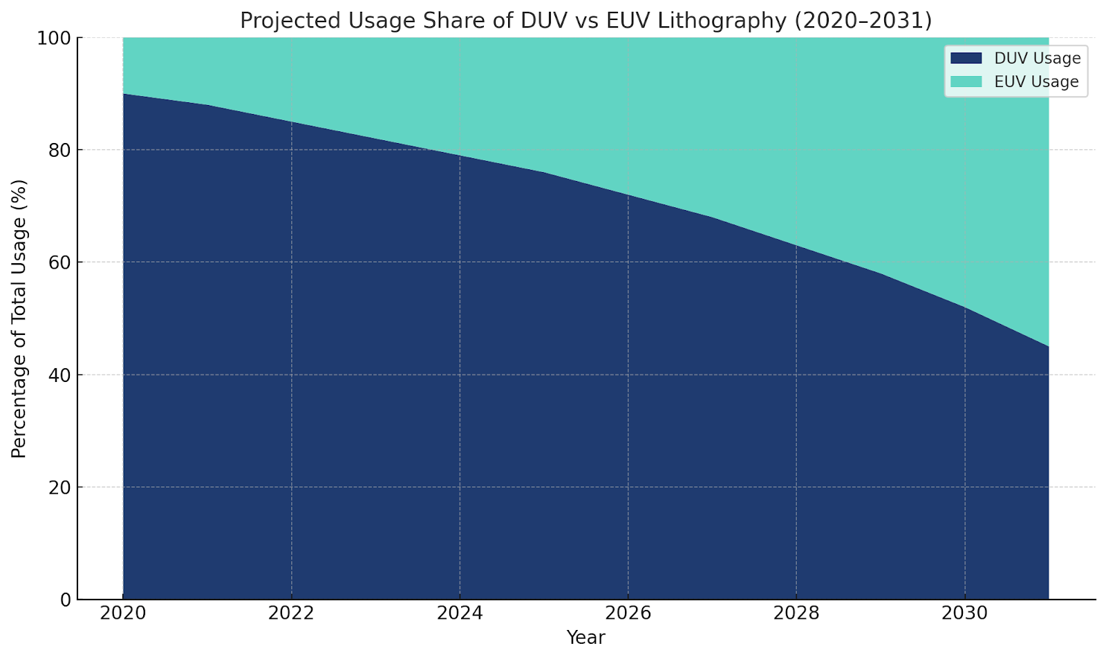
- DUV lithography currently dominates global usage, accounting for around 90% in 2020.
- EUV is reserved for advanced-node chips where every nanometer of performance and power efficiency matters.
- However, by 2031, EUV is projected to represent over 50% of lithography usage, catching up as more fabs shift to 5 nm, 3 nm, and eventually 2 nm processes.
Understanding how DUV and EUV work is only part of the picture. What’s just as important and often overlooked is what it actually takes to sell and deploy these machines inside a working fab. Unlike most industrial equipment, lithography tools are incredibly complex, expensive, and deeply embedded in the chipmaking process. Getting one installed at a leading fab is as much about trust, timelines, and technical integration as it is about the machine itself.
Why Selling Lithography Tools Is a Long Game
Selling a lithography machine, especially something as advanced as an EUV or high-NA EUV system isn’t like selling regular industrial equipment. These are among the most expensive, complex, and strategically sensitive machines in the entire semiconductor manufacturing process.
An EUV tool from ASML typically costs between $150–180 million, and the next generation of high-NA machines is expected to cross $300 million per unit. But price alone doesn’t capture the complexity involved.
What really makes these sales challenging is how long and involved the process is. Once a fab buys a lithography tool, it can take 6 to 12 months just to get it up and running. This includes detailed setup, testing, and making sure it works perfectly with the fab’s environment.
Even after installation, the machine becomes deeply embedded in the fab’s production process from how chips are patterned to how yields are optimized. It’s not something you can easily unplug and replace. In fact, many toolmakers send dedicated engineers to work onsite, helping fab teams operate and maintain the machine over the long term. After all that, switching to a new supplier isn’t just expensive, it’s risky and disruptive. It’s not just about the tool itself anymore, it’s about years of trust, tuning, and custom processes built around that specific machine. That’s why this market is so concentrated.
Source: https://www.asml.com/en/investors/financial-results
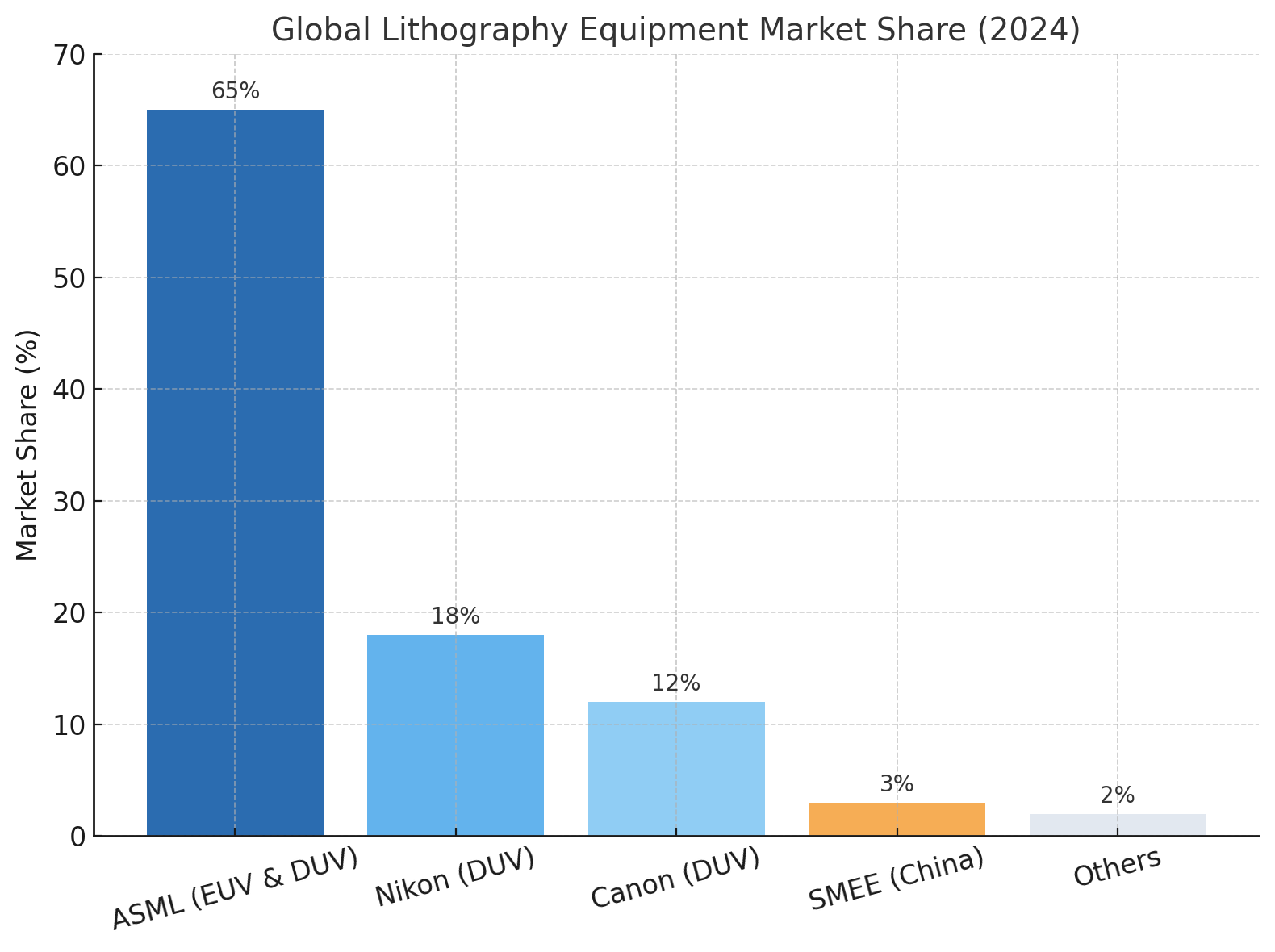
ASML dominates EUV, and Canon and Nikon remain strong in DUV, not just because of superior engineering, but because they’ve built long-term relationships and proven reliability in real-world manufacturing environments. It’s also why startups rarely attempt to build full lithography tools. The barriers aren’t just technical or financial rather they’re tied to trust, time, and deep process integration.
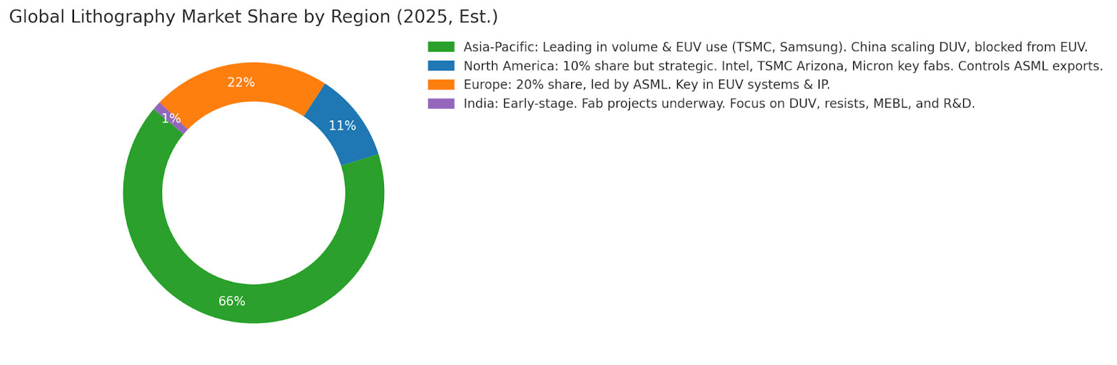
The Global Lithography Landscape
The global lithography equipment market is set to more than double over the next decade, growing from an estimated $29.26 billion in 2025 to around $65.31 billion by 2035 at a compound annual growth rate (CAGR) of ~7.6%.
North America makes up about 10% of the global lithography market, but the U.S. plays a key strategic role. It's home to chipmakers like Intel, Micron, NVIDIA, and AMD, and leads in R&D, advanced packaging, and high-performance chip design.
Through the CHIPS and Science Act, the U.S. is investing $50B+ to boost domestic semiconductor manufacturing — supporting fabs, tools, and talent. Companies like Intel (2 nm with high-NA EUV), TSMC Arizona (advanced chips for Apple), and Micron (DUV for memory) are leading adopters.
While the U.S. doesn’t build EUV systems, it remains central to the supply chain and even exerts export control over ASML, blocking EUV shipments to China.
Asia-Pacific holds over 60% of the global lithography market, led by China, Taiwan, South Korea, and Japan. The region hosts the world’s largest and most advanced fabs — including TSMC and Samsung, both major EUV users.
China is rapidly scaling mature-node capacity and investing in domestic alternatives like SMEE’s DUV tools, while being blocked from EUV access due to the U.S .- Dutch export restrictions. Japan remains key in DUV tool manufacturing (Canon, Nikon) and photoresist materials.
Asia isn’t just dominant in fab volume, but it’s actively working to localize lithography tech, especially as geopolitical tensions reshape global supply chains.
Source: https://www.semiconductors.org/resources/
India as of today has no commercial-scale semiconductor fabrication plant but there are many upcoming projects and JVs to build India’s first commercial fab such as Tata-PSMC and Micron, focused on 28–90 nm nodes using DUV tools.
With support from the $10B Indian Semiconductor Mission, the country is prioritizing materials, R&D, and fab-adjacent innovation. Academic institutions are leading the way — IIT Mandi, in collaboration with Lawrence Berkeley Lab, has demonstrated promising 20 nm EUV photoresists, while the University of Mumbai has developed a laser-based litho system for MEMS applications. Government labs like SCL Mohali and SAC Ahmedabad are working on legacy-node process R&D.
What’s Next in Lithography Innovation?
High-NA EUV is the most anticipated upgrade. It improves resolution from 13.5 nm to around 8 nm, allowing chipmakers to cut down on complex multi-patterning steps. ASML’s EXE:5000 systems, which bring this capability to market, are expected to be deployed starting in 2025–26.
Another promising path is Multicolumn Electron Beam Lithography (MEBL), which is a maskless, direct-write approach that uses hundreds of parallel electron beams. It’s not yet ready for high-volume production, but it holds strong potential for advanced packaging, prototyping, and R&D.
Meanwhile, materials innovation continues behind the scenes. New resists are being designed to withstand higher light doses and enable better pattern control at smaller nodes. This is one area where countries like India could contribute, given the capital-efficient nature of resist R&D.
Software is also becoming a key differentiator. As defects and overlay errors grow harder to manage at advanced nodes, AI is being used to optimize lithography steps — predicting pattern failures, tuning exposure settings, and enabling real-time metrology.
Finally, China is investing heavily in homegrown alternatives to EUV, since access to ASML systems remains blocked. State-backed research institutes are developing plasma-based EUV systems, using alternative laser-pulsed plasma sources. While these efforts are still years behind in maturity, they reflect a long-term national commitment to EUV self-sufficiency.
Our View at Speciale Invest
The lithography ecosystem sits at the heart of semiconductor manufacturing and is one of the most technically challenging and capital-intensive spaces in the industry. Only a handful of companies globally, like ASML, Nikon, and Canon, are capable of building full-stack lithography systems today. Entering that tier is a long, tedious process.
At Speciale Invest, we’re closely watching the lithography space and the layers surrounding lithography, i.e. in materials, sensing, metrology, and software and actively looking to back ambitious, capital-efficient, R&D-driven teams solving problems in these high-leverage areas. As India begins to build out its domestic semiconductor capacity, we believe these innovations can not only serve local fabs, but also scale globally as modular, fab-adjacent IP that plugs into the international supply chain.
References
- KBV Research – Global Lithography Equipment Market Size, 2020–2031
- Mordor Intelligence – Semiconductor Lithography Equipment Market Report
- IMARC Group – Global Lithography Systems Market Report
- ASML Investor Relations - Annual Reports
- SIA (Semiconductor Industry Association)- Reports
- BCG - Reports on semiconductor supply chains
- McKinsey - Reports on semiconductor supply chains
- European Commission - Reports on EU Chips Act
- Indian Semiconductor Mission (MeitY) - Economic Times Report
- Nature Electronics, IEEE Xplore, and SPIE Publications
- TechCrunch, EE Times, SemiWiki, and Nikkei Asia
